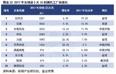
Very Large-Scale Integration (VLSI) design is a cornerstone of modern electronics, enabling the integration of millions to billions of transistors on a single silicon chip. This article provides a foundational overview of VLSI design principles, methodologies, and challenges, focusing on design flow and verification.
The VLSI design process typically follows a structured flow: specification, architectural design, logic design, circuit design, physical design, and fabrication. At the specification stage, requirements such as functionality, power consumption, speed, and area are defined. A crucial goal is to achieve low power dissipation with high reliability.
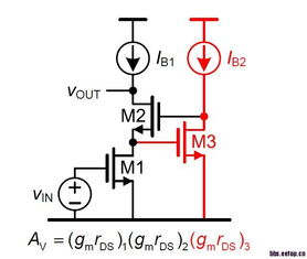
Digital VLSI design involves building logic gates, flip-flops, and more complex modules, often using Hardware Description Languages (HDLs) like Verilog or VHDL. Design optimization targets three main axes: power, performance, and area (PPA). Automation tools assist in steps such as synthesis and placement-and-routing (PnR). Verification mechanisms, including simulation and Formal Mathematical Proofs, play a critical input role to validate logic against Specifications found fundamental phases: with Clock and Power Implementation inserted especially Phase delay Timing closures heavily rely tailored Constraints.
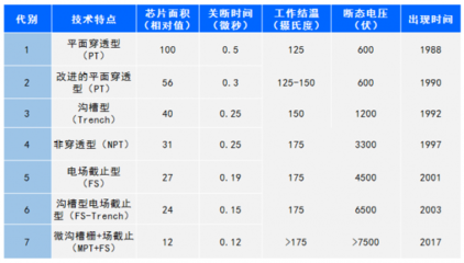
Analog and mixed-signal design present more difficulties, including noise marginalities and device characteristics process variation during crafting: Technology nodes below 5nmand continual industry cross disciplinary efforts catalyze unprecedented integration embedded chip bio growth necessary extending many compact betterment technical ability progress tasks broad yield field.